The Texting Typewriter (hardware)
This is my first blog post documenting the present state of my texting typewriter –and my first blog post ever. In future posts I will document both past and present work on this project, plus lots of other projects. This is my eleventh year teaching Engineering and Robotics at Medford Vocational Technical High School. Please check out my shop and student’s projects here. This post was also featured on Hackaday
The typewriter is a mid-80’s Panasonic T36 that can receive SMS messages. and print them along with the time of the message and the name of the sender. I have designed a generic hardware circuit that should be compatible with any electric typewriter (I will be testing a Brother AX-350 shortly). The interface to the control circuit is through a simple I2C connection. Presently an ESP32 handles all of the software including receiving the SMS message, file retrieval for the “address book” and sending control data to the typewriter circuit. Also, the paper is feed from an “infinite” roll of 11 inch wide typing paper, which for storage life beats magnetic tape by about half a millennia.
In addition to basic typing the circuit allows for simultaneous key presses which allows me to use SHIFT instead of CAPS LOCK, and the CODE key to set and clear bold text, underlined text, auto carriage return, text centering, flush right margin, setting and removing tabs and margins. With the AX-350 I expect to add pitch and line spacing.
I will also be adding a keyboard to the circuit to allow me to reply to text messages. Note: I don’t own a cell phone, so this is small compromise with the inevitable future!
Keyboard Interface: While there a few possibilities for interfacing with the typewriter, I chose to directly replace the keyboard inputs with control hardware. Below is an image of the keyboard and its internal circuit.

Above you can see that the keyboard circuit is made up of two layers. On the left side of each layer is ribbon cable that ends in twelve pins each. You can imagine the two layers as a set of rows and columns as depicted below and the button presses, connected one row to one column.

The ribbon cables themselves are inserted into two headers on the typewriters circuit board. When any key is pressed on the keyboard, a connection is made between one of the twelve pins on one header and one of the twelve pins on the other header causing that key to be typed on the typewriter, as demonstrated in the diagram below.

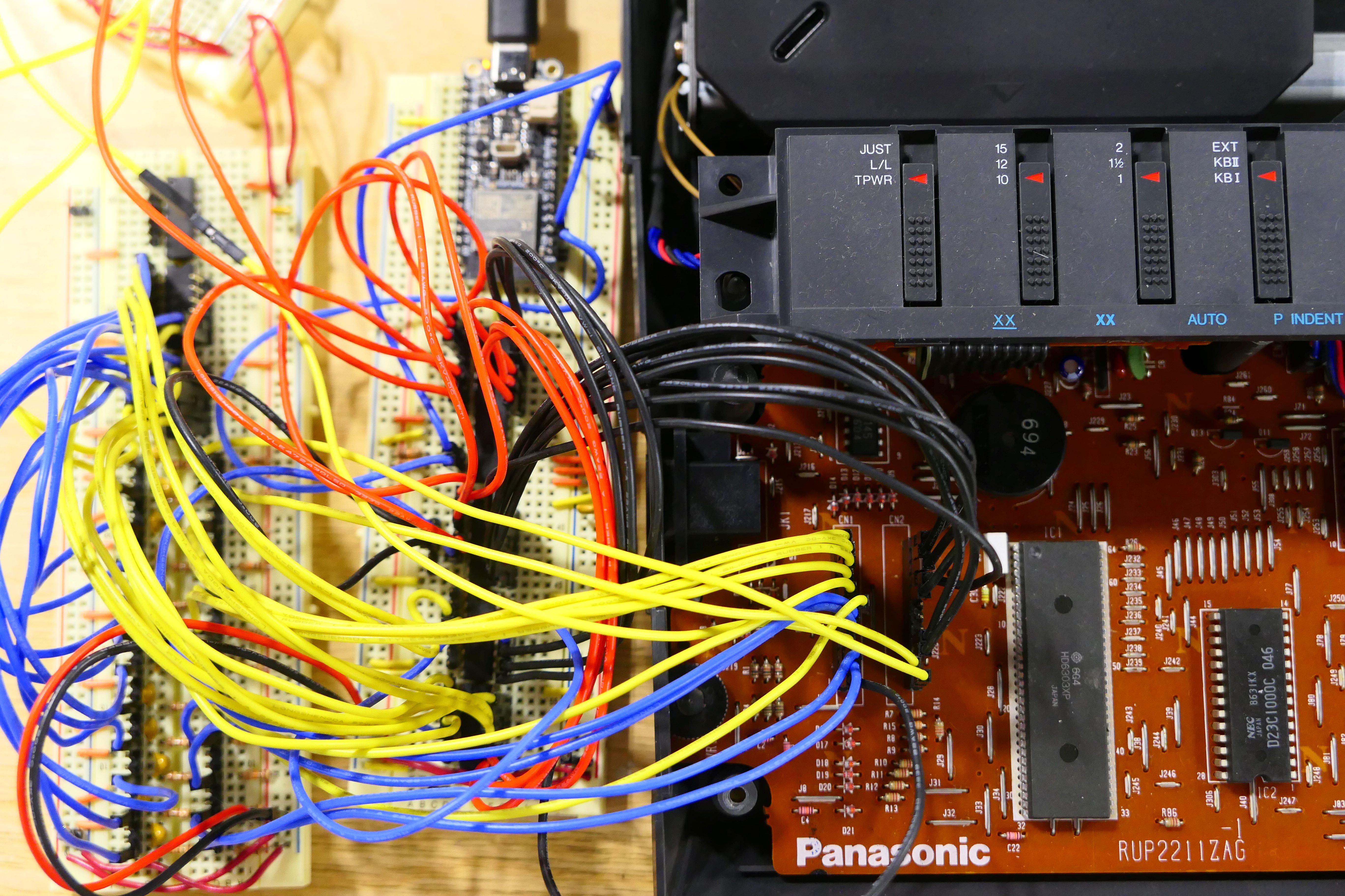
Below is an image of the actual typewriter circuit board. You can see the ribbon headers on the left side. On this board they have been replaced with pin headers to allow the use of jumper wires. Using jumper wires it is possible to type any key on the typewriter by shorting the pin from one header to the other.

The first question is how does the typewriter know which pin on header A is connected to which pin on header B. For example, how does pin three on header A know that it is connected to pin six of header B and not pin four of header B. The answer is that the pins on header B* are sending separately timed pulses, so the receiving pins on header A can determine which pin on header B is connected as detailed in the diagram below which includes a block showing my custom control circuit which takes care of the routing of the pins on one header to the other.

*It would have been nice if the two twelve pin headers on the typewriter circuit board lined up neatly with twelve column inputs and twelve row outputs, but that is not the case. I believe that when designing single sided circuit boards. trace management took priority over logical layout. Not that there are actually thirteen signal pins and eight receiving pins, but we can ignore those details for the moment.
The job of routing signals from one header to the other is accomplished by using multiplexer to select a signal pin and a demultiplexer to assign that signal to a scanning pin as shown in the overall diagram below.

Section A: This section represents the low band pass filter through which all signals pass. Originally, I found a small spike in the pulse lines that was getting interpreted as a full logic signal in the control logic. Using an RC bandpass filter, I was able to remove this spike. I would show a picture of this spike on the scope, but unfortunately (or fortunately) I am unable to recreate it on either typewriter. It was also going to be a good demonstration for my students. Be that as it may, the filters are there in case a future typewriter exhibits this behavior.
The signals also pass through a pair of 74HC14 Hex Schmitt−Trigger Inverters. Again a precautionary measure to make sure the signals are “clean” coming out of the band pass filter, but these might be removed in the final version.
Section B: In this section eleven of the thirteen pulse pins are channeled into two 74HC151 8-input multiplexers. A single 16-input would be more efficient, but I had two of these on hand and I was able to effectively “cascade” them together so that using a single address, I can select any one of the eleven pulse inputs. Each multiplexer is addressed using three address pins and both enables are held active.
Section C: The de-multiplexer is a 74HC138 1−of−8 Demultiplexer which can easily handle the seven SCANNING PINS A. The demultiplexer has three address pins and one chip select pin that can be used as an enable.
Section D: The pins controlling SHIFT and CODE are routed separately. Since these keys need to be pressed simultaneously with other keys, they cannot be handled by the multiplexer scheme. These pins are connected via a 74HC4066 Quadruple Bilateral Analog Switch. This IC has four bidirectional switches each controlled by a single pin. Each pulse pin is only matched with one scan pin so this solution can work for up to four command keys.
Section E: The entire routing circuit is controlled by a MCP23017 16-Bit I2C I/O Expander. This IC controls the whole circuit by addressing the multiplexer, de-multiplexer, and quad switch. It receives commands via I2C so it can be controlled by just about any microcontroller. In this case it is an ESP32.

Rational: This circuit design evolved from an earlier version I made a few a years ago. The original version used an Arduino to control the typewriter without any additional circuit interface. This design only used one signal input from the typewriter. In addition to the single pulse inputs, one of the pulse pins doubles a clock input. By monitoring the start pulse, the Arduino was able to fairly successfully mimic the correct pulse on the scanning pins. Occasional the typewriter printed stray characters…due to gremlins in the typewriter hardware. Designing a complete hardware solution allows the control circuit to be used with just about any electric typewriter regardless of timing schemes.
The original version also left the SMS portion of the project up to a Raspberry Pi which communicated with the Arduino through serial. This created the problem of having two devices and with code to maintain on both devices. Also serial communication with the Arduino is limited by the 64 byte buffer –shorter than the accepted limit for an SMS message. While this can be increased, it is just another problem.
The ESP32 can easily manage SMS messages. It has decent file management to store and retrieve phone numbers and names. By pushing the hardware control to the control circuit, the ESP32 only needs to communicate address via I2C to the control circuit.

Check out Part 2 to learn about the software developed for this project.